The conventional two-dimensional approach to bespoke PCB board design is no longer enough for many contemporary applications in the quickly changing electronics world of today. Engineers and designers are using vertical board layouts and 3D PCB design methodologies to optimize space utilization and enhance overall system performance as devices get more feature-rich and compact. This change marks a substantial advancement in their methodology for PCB design board solutions, especially in intricate electronic systems where space optimization is essential.
Comprehending Vertical Board Configurations
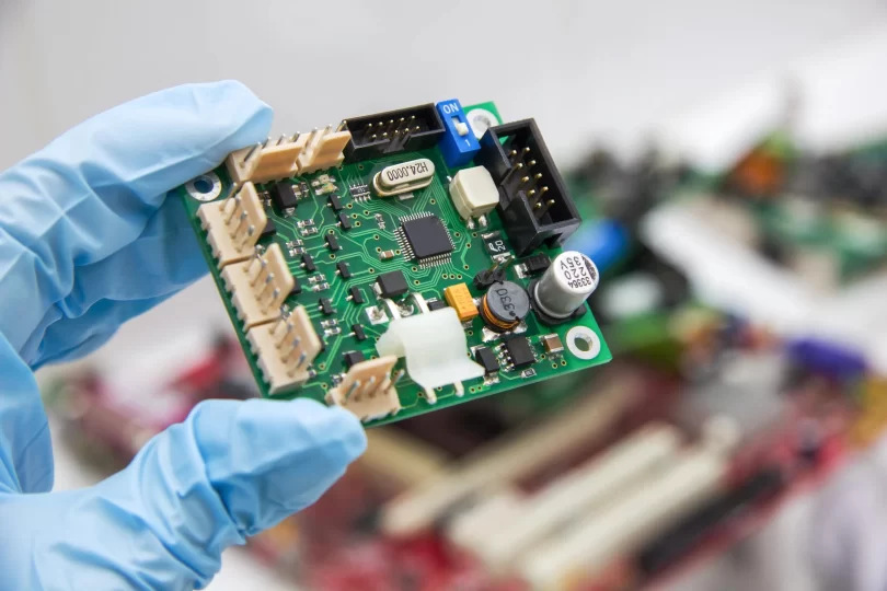
A significant change in the paradigm of custom PCB board design is represented by vertical board layouts. This method uses the vertical dimension to stack and arrange circuit boards in three-dimensional designs instead of distributing components across a single plane. In contemporary vlsi design processes, where the need for shrinking keeps spurring innovation in the creation of electronic products, this technique has grown in importance.
PCBs arranged vertically have a number of clear advantages over conventional horizontal layouts. Designers can preserve or even enhance functionality while drastically lowering the overall footprint of their electronic devices by leveraging the z-axis. Applications where space is a major problem, such industrial control equipment, automotive systems, and portable gadgets, benefit greatly from this strategy.
Important Things to Think About When Implementing 3D PCBs
Several important things need to be thoroughly considered before starting a 3D PCB design job. Because heat dissipation patterns in vertical layouts differ greatly from those in conventional horizontal designs, thermal management becomes more complicated. The thermal interaction between stacked boards must be taken into account by engineers when implementing suitable cooling solutions, such as thermal management components or strategically placed ventilation channels.
Another important factor to take into account while implementing vertical PCBs is signal integrity. There is a greater chance of electromagnetic interference when boards are stacked closer together. This calls for close consideration of signal routing plans, shielding methods, and component placement. To guarantee dependable operation of the finished product, these variables must be taken into consideration in the design of the custom PCB board.
In vertical board layouts, mechanical issues are also very important. All components must be adequately supported by the physical structure, which also ensures that the boards are properly aligned. This frequently calls both creative mounting techniques and meticulous attention to mechanical stress areas across the unit.
Top Techniques for 3D PCB Design
Following a number of PCB design board methodology best practices is necessary for the successful deployment of vertical board layouts. In 3D systems, component placement becomes especially important. Sensitive components need to be sufficiently protected from any interference sources, and high-heat generating components should be positioned strategically to maximize thermal dissipation.
In vertical designs, interconnection strategies are essential. In order to preserve signal integrity and reduce signal path lengths, board-to-board connections need to be carefully arranged. This could entail the application of flexible circuits, specialized connectors, or other creative connection techniques that take into account the three-dimensional structure while maintaining dependable electrical performance.
When working with high-density, multi-layer boards in vertical designs, the application of VLSI design principles becomes even more crucial. Working with intricate three-dimensional structures makes proper layer stackup planning and signal routing even more important. The requirements for power distribution, temperature control, and signal integrity must be carefully balanced throughout all of the assembly’s layers and boards by engineers.
Technologies and Tools for 3D PCB Design
In order to accommodate the growing complexity of three-dimensional layouts, modern PCB design tools have developed. Designers can now assess their custom PCB board designs from all perspectives and spot possible problems before going into production thanks to advanced CAD software’s advanced 3D visualization features. Features for evaluating mechanical stress, signal integrity, and thermal performance in three-dimensional topologies are frequently included in these instruments.
The ability to simulate has grown in significance during the design phase. Early in the development cycle, engineers can now discover and fix possible problems by simulating the electrical and thermal performance of their designs in three dimensions. When working with intricate vertical layouts, where actual prototypes could be expensive or time-consuming, this capacity is especially helpful.
Factors Affecting Vertical Layout Manufacturing
Assembly methods and procedures must be carefully considered during the design to manufacturing transition. Custom fixtures or tools may be needed for vertical board layouts, which frequently call for specific assembly techniques. To guarantee that every component can be positioned and soldered correctly and that quality control procedures can be carried out successfully, the production process needs to be meticulously designed.
Three-dimensional designs also require modifications to testing and validation protocols. To guarantee that the finished assembly can be adequately tested and maintained, access to test points and debugging interfaces must be taken into account during the design phase. This could entail using specialized testing equipment made for vertical board designs or putting in place particular test access points.
Future Trends and Applications
Applications for vertical board layouts can be found in many different product categories and sectors. In consumer electronics, this strategy enables the development of increasingly compact and feature-rich gadgets. Industrial applications benefit from the capacity to cram more functionality into constrained space envelopes, while automotive systems employ vertical designs to accommodate complex electronic systems within tight physical limitations.
PCB design board technology is still developing, and new trends suggest that three-dimensional design ideas will be included even more. Engineers’ approaches to vertical board layouts are starting to change as a result of advanced manufacturing techniques including embedded components and 3D-printed circuits. The potential for complex electronic systems in small form factors is expected to increase as a result of these breakthroughs.
Conclusion
Electronic product development has advanced significantly with the use of vertical board layouts and 3D PCB design approaches. Understanding these design techniques is becoming more and more crucial as technology develops and the need for small, powerful electronic devices increases. A deep comprehension of both conventional PCB design principles and the particular difficulties posed by three-dimensional designs is necessary for success in this field.
The many elements that affect the performance of vertical board layouts, ranging from mechanical stability and manufacturing viability to thermal management and signal integrity, must be carefully taken into account by engineers and designers. They may produce dependable and effective bespoke PCB board solutions that satisfy the exacting specifications of current electrical goods by adhering to accepted best practices and utilizing cutting-edge design tools.